 |
|||||||||||||
| RhinoPower | Hardware | Software | Forum | Tech | Contact | ||||||||
A summary of the features of the 76xxx Processors
Introduction
Over a number of years of reverse engineering ECUs I have determined that there are
many Japanese ECUs that use a processor/microcontroller family numbered 76xxxx, the evidence
points to these processors being manufactured by Toshiba.
I have never found any documentation for these devices and this document has been prepared
from information gleaned from bench
testing, code analysis and from the work carried out on the 76C75 (AKA MH6111) by Bill
Sundahl and others on the, now lost forever, DSM Yahoo group.
This is the nearest thing to a datasheet that there is on the internet but the information has been gleaned from reverse engineering and not from the manufacturer's datasheet. Signal and register names are my own using Motorola/Hitachi nomenclature. No claims are made for accuracy, use the data with caution and at your own risk, please do contact me if you have any further information or corrections.
The 76xxx processor is an evolution of the Hitachi HD6301 processor core used in some earlier ECUs. The HD6301 core has been extended with an additional index register (Y), extra timing functions have been added and the instruction set greatly extended. The 40-pin DIL variants have a pinout compatible with the 6301 and the Motorola 6801 processor, indeed an Aisin Warner TCM uses only 6801 instructions, ignoring the Y-indexing and additional op-codes completely; the larger packages have unique pin outs. An interesting point to note is that although the lower part of the register set is backwardly compatible with the 40-pin HD6301V the upper registers are not the same, nor are the timers compatible with those of the larger 6301 packages.
For development and testing I am using MGTEK MiniIDE with the Telemark TASM assembler using a modified op-code table, however it is possiblt to use any hc11 compiler if only 6801 instructions are used. I have a Windows based disassembler in development and there are instructions on how to setup MiniIDE here.
Processor Variants
Below is a list of known variants please email me if you know of any others.
| Variant | Package | Marking | Image |
|---|---|---|---|
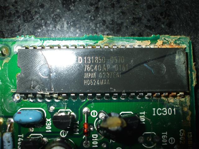
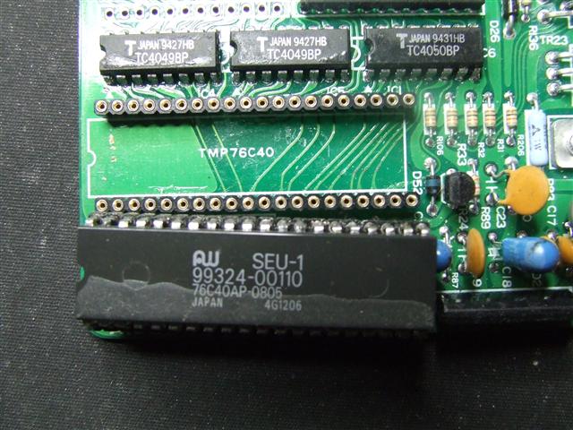
| 76C40AP | 40-pin DIL | Various used by Denso and Aisin Warner | Image 1 Image 2 |
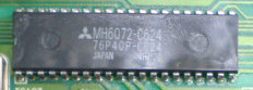
| 76P40AP | 40-pin DIL | MH6072 Mitsubishi | Image 1 |
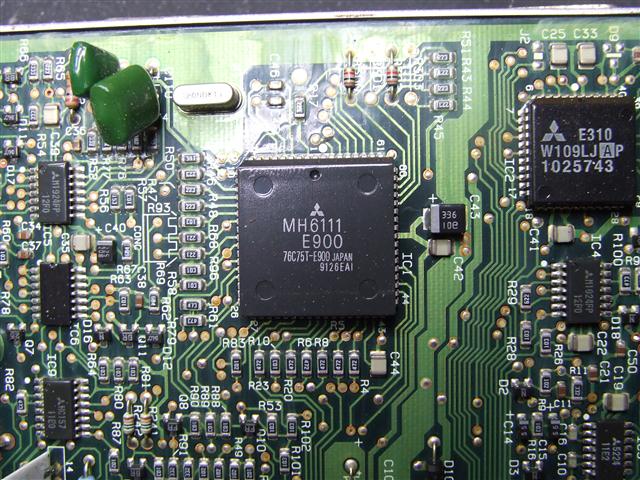
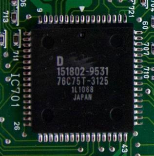
| 76C75T | 68-pin PLCC | Various used by Mitsubishi(MH6111),Denso and others | Image 1 Image 2 |
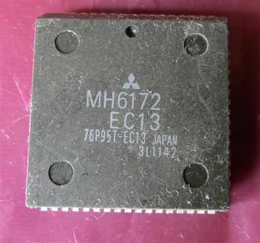
| 76P95T | 68-pin PLCC | MH6172 Mitsubishi | Image 1 |
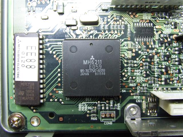
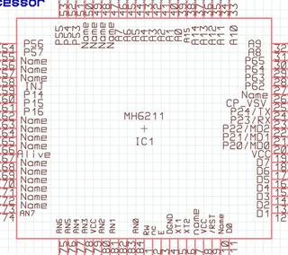
| 76C175AT | 84-pin PLCC | MH6211 Mitsubishi | Image 1 |
| 76C55T | 84-pin PLCC | MH6311 Mitsubishi | No image |
| 76C55AF | 100-pin TQFP | MH6311 Mitsubishi | Image 1 |
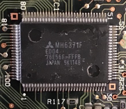
| 76E56AF | 100-pin TQFP | MH6371 Mitsubishi | Image 1 |
Package details
Processor pin-outs
This is very much a work in progress not all pin outs are known.
| Pin | 40-pin | 68-pin | 84-pin | 100-pin | |
|---|---|---|---|---|---|
| Mode | Expanded multiplexed | Single Chip | Expanded multiplexed | Expanded non-multiplexed | Expanded non-multiplexed |
| 1 | GND | RW | RW | RW | |
| 2 | XTAL | AS | AS | AS | A5 |
| 3 | EXTAL | E | E | E | |
| 4 | nNMI | GND | GND | GND | |
| 5 | nIRQ | XTAL1 | XTAL1 | XTAL1 | A6 |
| 6 | nRESET | XTAL2 | XTAL2 | XTAL2 | A7 |
| 7 | VCC | nNMI | A8 | ||
| 8 | P20/MD0 | 5V | 5V | 5V | A9 |
| 9 | P21/MD1 | nReset | A10 | ||
| 10 | P22/MD2 | nRESET | nRESET | nHalt | A11 |
| 11 | P23 | VCC | VCC | D0 | A12 |
| 12 | P24 | D1 | A13 | ||
| 13 | P10 | D2 | A14 | ||
| 14 | P11 | P22/OC1 | P22/OC1 | D3 | |
| 15 | P12 | P23/RX | P23/RX | D4 | |
| 16 | P13 | P24/TX | P24/TX | D5 | |
| 17 | P14 | D6 | P75 | ||
| 18 | P15 | P10/IC1 | P10/IC1 | D7 | P74? |
| 19 | P16 | P11/OC2 | P11/OC2 | 5V | P73? |
| 20 | P17 | P12/OC3 | P12/OC3 | P20/MD0 | P72? |
| 21 | VCC stdby | P13/OC4 | P13/OC4 | P21/MD1 | P71? |
| 22 | A15 | P14 | P14 | P22/MD2/OC1? | P70? |
| 23 | A14 | P15 | P15 | P23/RX | VCC |
| 24 | A13 | P16 | P16 | P24/TX | 0V |
| 25 | A12 | P17/PAI | P17/PAI | P25?/P61? | |
| 26 | A11 | n.c. | AN0 | ||
| 27 | A10 | P60 | P60 | P62 | |
| 28 | A9 | P61 | P61 | P63 | |
| 29 | A8 | P62 | P62 | P64 | AN1 |
| 30 | AD7 | P63 | P63 | P65 | |
| 31 | AD6 | P64 | P64 | AD8 | AN2 |
| 32 | AD5 | P65 | P65 | A9 | AN3 |
| 33 | AD4 | A10 | AN4 | ||
| 34 | AD3 | AN7 | AN7 | A11 | AN5 |
| 35 | AD2 | AN6 | AN6 | A12 | AN6 |
| 36 | AD1 | AN5 | AN5 | A13 | AN7 |
| 37 | AD0 | AN4 | AN4 | A14 | AN8? |
| 38 | R/W | AN3? | AN3? | A15 | AN9? |
| 39 | AS | AN2? | AN2? | A0 | |
| 40 | E | AN1? | AN1? | A1 | |
| 41 | AN0? | AN0? | A2 | ||
| 42 | 0VA | 0VA | A3 | R/~W | |
| 43 | 5VA | 5VA | A4 | E | |
| 44 | P57 | P57 | A5 | ||
| 45 | P56 | P56 | A6 | XTAL1 | |
| 46 | P55 | P55 | A7 | XTAL2 | |
| 47 | P54 | P54 | GND | ||
| 48 | P53 | P53 | P50? | ||
| 49 | P52/OC? | P52/OC? | P51? | ||
| 50 | P51 | P51 | P52? | ||
| 51 | P50 | P50 | P53 | ||
| 52 | VCC | VCC | P54 | D0 | |
| 53 | P47 | A15 | P55 | ||
| 54 | P46 | A14 | P56 | ||
| 55 | P45 | A13 | P57 | D1 | |
| 56 | P44 | A12 | P10 | D2 | |
| 57 | P43 | A11 | OC2/P11 | D3 | |
| 58 | P42 | A10 | OC3/P12 | D4 | |
| 59 | P41 | A9 | OC4/P13 | D5 | |
| 60 | P40 | A8 | P14 | D6 | |
| 61 | P37 | AD7 | P15 | D7 | |
| 62 | P36 | AD6 | P16 | 5V? | |
| 63 | P35 | AD5 | P17? | P20? | |
| 64 | P34 | AD4 | GND | P21 | |
| 65 | P33 | AD3 | GND | P22/SCK | |
| 66 | P32 | AD2 | GND | ||
| 67 | P31 | AD1 | ? | P23/RX | |
| 68 | P30 | AD0 | ? | P24/TX | |
| 69 | 5V | P10 | |||
| 70 | GND | P11 | |||
| 71 | 5VA? | P12 | |||
| 72 | 5V | P13 | |||
| 73 | GND | P14 | |||
| 74 | AN7 | P15 | |||
| 75 | AN6 | P16 | |||
| 76 | AN5 | P17 | |||
| 77 | AN4 | ||||
| 78 | AN3? | ||||
| 79 | AN2? | P57 | |||
| 80 | AN1 | ||||
| 81 | AN0 | P56 | |||
| 82 | 5V | P55 | |||
| 83 | n.c. | P54 | |||
| 84 | Pulled up to 5V | P53 | |||
| 85 | P52 | ||||
| 86 | P51 | ||||
| 87 | P50? | ||||
| 88 | |||||
| 89 | |||||
| 90 | |||||
| 91 | |||||
| 92 | |||||
| 93 | |||||
| 94 | |||||
| 95 | |||||
| 96 | A0 | ||||
| 97 | A1 | ||||
| 98 | A2 | ||||
| 99 | A3 | ||||
| 100 | A4 | ||||
Register Maps - Except 100-pin devices
The 76XXX has a memory map that clearly shows its 6301 origins with
control registers and ports located in the first 31 addresses. The first 20
addresses are identical to the 6301 but note that above address 31 the functions
appear similar to the 6303, the 6301's 'big brother', but the memory mapping is
different and the timer modules have different functionality and appear to have
been designed specifically for engine management.
RAM is located from address 40h upwards.
RAM is located from address 40h upwards.
| Address | Name | Function |
|---|---|---|
| -------- 6301/6801 Compatible Registers -------- | ||
| 00 | PORT1DDR | PORT1 Data Direction Register |
| 01 | PORT2DDR | PORT2 Data Direction Register |
| 02 | PORT1 | PORT1 Data Register |
| 03 | PORT2 | PORT2 Data Register |
| 04 | P3DDR | PORT3 Data Direction Register |
| 05 | P4DDR | PORT4 Data Direction Register |
| 06 | PORT3 | PORT3 Data Register |
| 07 | PORT4 | PORT4 Data Register |
| 08 | T1CSR1 | Timer1 Control and Status Register 1 |
| 09 | TMR1H | Timer 1 - Free Running Counter High Byte |
| 0A | TMR1L | Timer 1 - Free Running Counter Low Byte |
| 0B | T1OCR1H | Output Compare Register 1 High Byte |
| 0C | T1OCR1L | Timer1 Output Compare Register 1 Low Byte |
| 0D | T1ICR1H | Timer1 Input Capture Register 1 High Byte |
| 0E | T1ICR1L | Timer1 Input Capture Register 1 Low Byte |
| 0F | P3CSR | PORT3 Control and Status Register |
| 10 | SCIRMC | SCI Rate and Mode Control Register |
| 11 | SCSR | SCI Control and Status Register |
| 12 | RXD | SCI Rx Data Register |
| 13 | TXD | SCI Tx Data Register |
| 14 | RAMCR | RAM Control Register |
| -------- 76XXX Specific Registers - all packages -------- | ||
| 15 | P5DDR | Port5 Data Direction Register |
| 16 | PORT5 | Port5 Data Register |
| 17 | ?? | Unused? |
| 18 | T1CSR2 | Timer1 Control and Status Register 2 |
| 19 | T2CSR2 | Timer2 Control and Status Register 1 |
| 1A | T2CSR2 | Timer2 Control and Status Register 2 |
| 1B | T1OCR2H | Timer1 Output Compare Register 2 High Byte |
| 1C | T1OCR2L | Timer1 Output Compare Register 2 Low Byte |
| 1D | T1ICR2H | Timer1 Input Capture Register 2 High Byte |
| 1E | T1ICR2L | Timer1 Input Capture Register 2 Low Byte |
| 1F | P6DDR ADCCTL |
Port6 DDR on 6211 ADC Control on 6111 |
| 20 | PORT6 ADCRES |
P6 on 6211 ADC Result on 6111 |
| 21 | ?? | Unused? |
| 22 | ?? | Unused? |
| 23 | ?? | Unused? |
| 24 | PACTL | Pulse Accumulator Control Register |
| 25 | PACNT | Pulse Accumulator Counter |
| 26 | RTICR | RTI Control Register |
| 27 | RTIFCR | RTI Frequency Control Register |
| 28 | ??? | Unused? |
| 29 | TMR2H | Timer 2 Free Running Counter High Byte |
| 2A | TMR2L | Timer 2 Free Running Counter Low Byte |
| 2B | T2OC3H | Timer2 Output Compare Register 3 High Byte |
| 2C | T2OC3L | Timer2 Output Compare Register 3 Low Byte |
| 2D | TMR3H? | Timer 3 Free Running Counter High Byte ? |
| 2E | TMR3L? | Timer 3 free Running Counter Low Byte ? |
| 2F | PORT6 | Port 6 Data Register |
| -------- 84-pin packages only -------- | ||
| 30 | P7DDR | Port7 Data Direction Register |
| 31 | PORT7 | Port7 Data Register |
| 32 | ----------- | ----------- |
| 33 | ----------- | ----------- |
| 34 | ----------- | ----------- |
| 35 | ----------- | ----------- |
| 36 | ----------- | ----------- |
| 37 | ----------- | ----------- |
| 38 | ADCCR | ADC Control Register |
| 39 | ----------- | ----------- |
| 3A | ----------- | ----------- |
| 3B | ----------- | ----------- |
| 3C | ----------- | ----------- |
| 3D | ADCDATA | ADC Data Register |
| 3E | ----------- | ----------- |
| 3F | ----------- | ???????????? |
| -------- Standby RAM -------- | ||
| ? | ----------- | ???????????? |
| -------- Volatile RAM -------- | ||
Register Map - 100-pin devices
The register map for the 76C55 (100-pin) is quite different from the smaller devices, currently it is a work in progress and can
be found here : 76C55 Register Map
PORTS
Data Direction Registers - 1=output, 0=input
Ports shared with other functions, ie timers, are generally read only, unless this is selectable in another register which hasn't yet been discovered (0Fh is unknown).
Ports shared with other functions, ie timers, are generally read only, unless this is selectable in another register which hasn't yet been discovered (0Fh is unknown).
Timers
Timer 1
Timer 1H, Timer1L - 09h:0Ah
This is a 16-bit Free running counter at 09h and 0Ah and is
driven by the E-clock (MH6211=4MHz). Its value can be set by writing a 16-bit word to
to 09h.
| 15 | 14 | 13 | 12 | 11 | 10 | 9 | 8 | 7 | 6 | 5 | 4 | 3 | 2 | 1 | 0 |
| Timer1H | Timer1L | ||||||||||||||
Timer 1 Control/Status Register 1 - 08h
| 7 | 6 | 5 | 4 | 3 | 2 | 1 | 0 |
| T1ICF1 | T1OCF1 | T1OIF | EICI1 | EOCI1 | T1OIE | IEDG1 | OLVL1 |
| bit7 | ICF1 - Input Capture Flag 1 | Set when an Input Capture 1 Event occurs |
| bit6 | OCF1 - Output Compare Flag 1 | Set when an Output Compare 1 event occurs |
| bit5 | OIF | Timer 1 overflow Interrupt flag |
| bit4 | EICIn - Enable Input Capture 1 Interrupt | Input Capture Interrupt 1 Enable |
| bit3 | EOC1I - Enable Output Compare 1 Interrupt | Set to enable an interrupt on output compare event |
| bit2 | OIE - Timer 1 Overflow Interrupt Enable | Set to enable |
| bit1 | IEDG1 - Input Edge Select 1 | This bit selects which edge causes an Input Capture
event 0=negative edge, 1=positive edge |
| bit0 | OLVL1 - Output Level 1 | This bit is transferred to P21/OC1 when an Output Compare 1 event occurs |
Timer 1 Output Compare 1 - 0Bh:0Ch
A match is generated when OCR1H:OCR1L = TMR1H:TMR1L, an interrupt will be generated if T1CSR1[EOC1I] is set. When a match
occurs the logic level at OLVL1 is transferred to ?????? (pin)
| 15 | 14 | 13 | 12 | 11 | 10 | 9 | 8 | 7 | 6 | 5 | 4 | 3 | 2 | 1 | 0 |
| T1OCR1H | T1OCR1L | ||||||||||||||
Timer 1 Input Capture 1 - 0Dh:0Eh
An event occurs when ??????? (pin) changes state if the polarity matches that defined by T1CSR1[IEDG1]. When an event does occur
occurs TMR1H:TMR1L is transferred to T1ICR1H:T1ICR2 and T1CSR1[T1IC1IF] is set. An interrupt will occur if T1CSR[T1IC1IE] is set.
| 15 | 14 | 13 | 12 | 11 | 10 | 9 | 8 | 7 | 6 | 5 | 4 | 3 | 2 | 1 | 0 |
| T1ICR1H | T1ICR1L | ||||||||||||||
Timer 1 Control/Status Register 2 - 18h
| 7 | 6 | 5 | 4 | 3 | 2 | 1 | 0 |
| ICF2 | OCF2 | OLVL4 | EICI2 | EOCI2 | OLVL3 | IEDG2 | OLVL2 |
| bit7 | ICF2 - Input Capture Flag 2 | Set when an Input Capture 2 Event occurs |
| bit6 | OCF2 - Output Compare Flag 2 | Set when an Output Compare 2 event occurs |
| bit5 | OLVL4 - Output Level 4 | This bit is transferred to P13/OC4 when an Output Compare event occurs |
| bit4 | EICI2 - Enable Input Capture Interrupt n | Input Capture Interrupt 2 Enable |
| bit3 | EOCI2 - Enable Output Compare 2 Interrupt | Set to enable an interrupt on output compare event |
| bit2 | OLVL3 - Output Level 3 | This bit is transferred to P12/OC3 when an Output Compare 2 event occurs |
| bit1 | IEDG2 - Input Edge Select 2 | This bit selects which edge causes an Input Capture
event 0=negative edge, 1=positive edge |
| bit0 | OLVL2 - Output Level 2 | This bit is transferred to P11/OC2 when an Output Compare 2 event occurs |
Timer 1 Output Compare 2 - 1Bh:1Ch
A match is generated when OC21H:OCR2L = TMR1H:TMR1L, an interrupt will be generated if T1CSR2[EOC2I] is set. When a match
occurs the logic level at OLVL2 is transferred to ?????? (pin)
| 15 | 14 | 13 | 12 | 11 | 10 | 9 | 8 | 7 | 6 | 5 | 4 | 3 | 2 | 1 | 0 |
| T1OCR2H | T1OCR2L | ||||||||||||||
Timer 1 Input Capture 2 - 1Dh:1Eh
An event occurs when ??????? (pin) changes state if the polarity matches that defined by T1CSR2[IEDG2]. When an event does occur
occurs TMR1H:TMR1L is transferred to T1ICR2H:T1ICR2L and T1CSR1[T1IC2IF] is set. An interrupt will occur if T1CSR2[IC2IE] is set.
| 15 | 14 | 13 | 12 | 11 | 10 | 9 | 8 | 7 | 6 | 5 | 4 | 3 | 2 | 1 | 0 |
| T1ICR2H | T1ICR2L | ||||||||||||||
Timer 2
Timer 2H, Timer2L - 29h,2Ah
This is a 16-bit Free running counter at 29h and 2Ah and is
driven by the E-clock (MH6211=4MHz). Its value can be set by writing a 16-bit word to
to 29h ????????
Timer 2 Control/Status Register 1 - 19h
This appears to be the CSR for more output compare functions in 1Ah, these functions use Timer 2
| 7 | 6 | 5 | 4 | 3 | 2 | 1 | 0 |
| ???? | ???? | ???? | ???? | ???? | ???? | ???? | ???? |
| bit7 | ??? | 0 on every loop t3_csr1 |
| bit6 | ??? | 1 on every loop |
| bit5 | ??? | 0 on every loop |
| bit4 | ??? | 1 on init but not on every loop, used to decide which of t3_clock1 or t3_clock2 should be used upon a CAS interrupt??? |
| bit3 | ??? | 1 Set to 0 when the output compare interrupt need to energize coil for cylinder 2 or 3, i.e. bit will be loaded in port5.2 when interrupt occur |
| bit2 | ??? | 1 Set to 0 when the output compare interrupt need to energize coil for cylinder 1 or 4, i.e. bit will be loaded in port5.1 when interrupt occur |
| bit1 | ??? | 1 on every loop |
| bit0 | ??? | 0 all the time except, set to 1 when no cas interrupt received for 1.275sec??? - timer2 overflow???? |
Timer 2 Control/Status Register 2 - 1Ah
This seems to contain output compare functions
| bit7 | ??? | 0 Input capture 1 |
| bit6 | ??? | 0 1 indicate that the outCompInt3 interrupt is pending/has been activated??? |
| bit5 | ??? | 0 |
| bit4 | ??? | 0 |
| bit3 | ??? | 1 Cylinder 1/4 or 2/3 ?? output compare detection polarity? |
| bit2 | ??? | 0 Cylinder 1/4 or 2/3 ?? output compare detection polarity? |
| bit1 | ??? | 1 Cylinder 1/4 or 2/3 ?? output compare detection polarity? |
| bit0 | ??? | 0 Cylinder 1/4 or 2/3 ?? output compare detection polarity? |
Pulse Accumulator
L0024, PACTL - PA Control Register
| bit7 | PAOVIF | Pulse Accumulator Interupt Flag |
| bit6 | ??? | ??? |
| bit5 | ??? | ??? |
| bit4 | PAOVIE | Pulse Accumulator Interrupt Enable |
| bit3 | ??? | ??? |
| bit2 | ??? | ??? |
| bit1 | ??? | ??? |
| bit0 | ??? | ??? |
L0025, PACNT - PA Counter
L0026 - RTI_CTRL1
Timer control and status register used for real time interrupt? init to $64 = 1.25ms?
| bit7 | ??? | ??? |
| bit6 | TIE | ??? |
| bit5 | ??? | ??? |
| bit4 | ??? | ??? |
| bit3 | ??? | ??? |
| bit2 | ??? | ??? |
| bit1 | ??? | ??? |
| bit0 | ??? | ??? |
L0027 - RTI_CTRL2?
Real time interrupt frequency setting: Freq = 125000/(256-x) where x is the content of rti_freq
L0028 - Unknown
Serial Communications Interface (SCI)
SCI Rate and Mode Control Register - 10h
| bit7 | 6 | 5 | 4 | 3 | 2 | 1 | bit0 |
| 7 | 6 | 5 | SS2 | CC1 | CC0 | SS1 | SS0 |
| bits 7:5 | Unimplemented? | |
| bits 4,1:0 | SS2:0 | Clock divider Clock divider 000=E/16, 001=E/128, 010=E/1024, 011=E/4096 |
| bits3:2 | CC | Mode Control bits 01 = Asyncronous mode, 8-bit, internal clk 10 = synchronous 8-bit, internal clock |
SCI Control and Status Register - 11h
| 7 | 6 | 5 | 4 | 3 | 2 | 1 | bit0 |
| RDRF | ORFE | TDRE | RIE | RE | TIE | TE | SWU |
| bit7 | RDRF - Rx Data Received | Set when data is present |
| bit6 | ORFE - Overrun or Framing Error | Set when a data overrun or framing error is detected |
| bit5 | TDRE - Transmit Data Register Empty | Set when TDR is empty |
| bit4 | RIE - Receiver Interrupt Enable | Set this bit to enable interrupts on data received |
| bit3 | RE - Receiver Enable | Set to enable TOF to generate an /IRQ2 interrupt? |
| bit2 | TIE - Transmit Interrupt Enable | set this bit to enable interrupt on transmit complete |
| bit1 | TE - Transmitter Enable | |
| bit0 | SWU - Wake Up |
RDR - Receive data Register - 12h
TDR - Transmit Data Register - 13h
Analogue to Digital Converter (ADC)
ADC Control Register 1Fh or 38h
| bit7 | - | ? |
| bit6 | - | ? |
| bit5 | - | Done - set to 1 when conversion complete |
| bit4 | - | Clock Control/Format Select |
| bit3 | GO | Start Bit set to 1 to start conversion |
| bit2-0 | C(2:0) | ADC channel number |
ADC Result Register 20h or 3Dh
8-bit unsigned ADC result
Interrupt Vectors
Interrupt vectors are located at the top of the 64k address range:
| FFD8h; | ||
| FFDAh | SCI | Serial Communications Interface RX or Tx |
| FFDCh | ||
| FFDEh | ||
| FFE0h | ||
| FFE2h | ||
| FFE4h | RTI | Real Time Interrupt |
| FFE6h | ||
| FFE8h; | ||
| FFEAh | T1OF | Timer 1 Overflow |
| FFECh | OC3 | Output Compare 3 |
| FFEEh | OC2 | Output Compare 2 |
| FFF0h | OC1 | Output Compare 1 |
| FFF2h | ??? | |
| FFF4h | Input Capture 2 | |
| FFF6h | Input Capture 1 | |
| FFF8h | nIRQ | External Masked Interrupt |
| FFFAh | SWI | Software Interrupt |
| FFFCh | nNMI | Not Masked External Interrupt |
| FFFEh | nReset | System Reset |
There is no apparent trap for invalid op-codes, the processor ignores any code that it doesn't recognise.
Instruction Set
The instruction set (this needs verifying) is available as a word document and can be downloaded here:
MH6211 Instruction Set
I have a few test programmes that are available for download, these programmes demonstrate the use of various functions. Note that these programmes were developed for use on Suzuki ECUs with a watchdog timer output on portx bitx. before running any programmes on your hardware you should check the configuration settings for compatibility. These programmes were compiled using the TASM assembler under MiniIDE.
| Demo1 | Simple I/O | Simple I/O |
| Demo2 | Serial Port and timers | Serial Port and timers |
| Demo3 | Advanced timer functions and interrupts | Advanced timer functions and interrupts |
| Demo4 | Analogue to Digital Conversion | Analogue to Digital Conversion |
Part Numbers
The 76xxx series appears to follows conventional Toshiba part numbering:
TMP = Toshiba MicroProcessor
76 = Processor series
C = Masked ROM, P = One Time programmable, E = EEPROM
75 = processor type
A = Enhanced
P = Plastic DIP, T = Plastic LCC, F = Plastic QFP
TMP = Toshiba MicroProcessor
76 = Processor series
C = Masked ROM, P = One Time programmable, E = EEPROM
75 = processor type
A = Enhanced
P = Plastic DIP, T = Plastic LCC, F = Plastic QFP
76xxx vs MC68HC11
It has been stated elsewhere that the 76xxx processor is a variant of the 68HC11, however this is clearly not correct.
These processors are an evolution of the 6301 as was the 68HC11 but they are a parallel development with obvious differences.
The instruction sets use different op-codes for many functions, primarily the
implementation of the Y index register, that means that HC11 software tools are
unsuitable for use with the 76xxx.
The processor registers are also mapped differently, with the HC11 defaulting to address 1000h and the 76xxx defaulting to or being fixed at address 0000h.
I have not seen any reference to an HC11 style bootloader implemented on the 76xxx although there is some evidence that there may be one on processors fitted to ECUs using an external EPROM, however this would be for loading firmware onto a pre-built board and there is no erase capability.